Sign In | Join Free | My burrillandco.com |
|
Ask Lasest Price | |
Brand Name : | ATMEL |
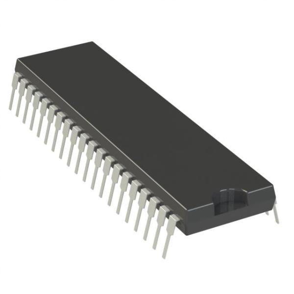
Model Number : | ATMEGA16A-PU |
Certification : | Original Factory Pack |
Price : | Negotiation |
Payment Terms : | T/T, Western Union,PayPal |
Supply Ability : | 5200PCS |
Delivery Time : | 1 Day |
Figure 6-1. Block Diagram of the AVR MCU Architecture
In order to maximize performance and parallelism, the AVR uses a Harvard architecture – with separate memories and buses for program and data. Instructions in the program memory are executed with a single level pipelining. While one instruction is being executed, the next instruction is pre-fetched from the program memory. This concept enables instructions to be executed in every clock cycle. The program memory is In-System Reprogrammable Flash memory. The fast-access Register File contains 32 x 8-bit general purpose working registers with a single clock cycle access time. This allows single-cycle Arithmetic Logic Unit (ALU) operation. In a typical ALU operation, two operands are output from the Register File, the operation is executed, and the result is stored back in the Register File – in one clock cycle.
. The Parallel Instruction Fetches and Instruction Executions
Reset and Interrupt Handling
The AVR provides several different interrupt sources. These interrupts and the separate reset vector each have a separate program vector in the program memory space. All interrupts are assigned individual enable bits which must be written logic one together with the Global Interrupt Enable bit in the Status Register in order to enable the interrupt. Depending on the Program Counter value, interrupts may be automatically disabled when Boot Lock bits BLB02 or BLB12 are programmed. This feature improves software security. See the section “Memory Programming” on page 264 for details.
![]() |