Sign In | Join Free | My burrillandco.com
Home > Amplifier >

Various Mosfet Power Transistor 6N60 Z 6.2A 600V Radio Amplifier Equivalent Marking

    Buy cheap Various Mosfet Power Transistor 6N60 Z 6.2A 600V Radio Amplifier Equivalent Marking from wholesalers
     
    Buy cheap Various Mosfet Power Transistor 6N60 Z 6.2A 600V Radio Amplifier Equivalent Marking from wholesalers
    • Buy cheap Various Mosfet Power Transistor 6N60 Z 6.2A 600V Radio Amplifier Equivalent Marking from wholesalers

    Various Mosfet Power Transistor 6N60 Z 6.2A 600V Radio Amplifier Equivalent Marking

    Ask Lasest Price
    Brand Name : Hua Xuan Yang
    Model Number : 6N60
    Certification : RoHS、SGS
    Price : Negotiated
    Payment Terms : L/C T/T Western Union
    Supply Ability : 18,000,000PCS / Per Day
    Delivery Time : 1 - 2 Weeks
    • Product Details
    • Company Profile

    Various Mosfet Power Transistor 6N60 Z 6.2A 600V Radio Amplifier Equivalent Marking

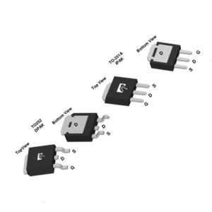
    6N60 Z 6.2A 600V N-CHANNEL POWER MOSFET


    DESCRIPTION

    The UTC 6N60Z is a high voltage power MOSFET and is designed to have better characteristics, such as fast switching time, low gate charge, low on-state resistance and high rugged avalanche characteristics. This power MOSFET is usually used at high speed switching applications in switching power supplies and adaptors.


    FEATURES

    RDS(ON) < 1.75Ω @ VGS = 10V, ID = 3.1A

    * Fast switching capability

    * Avalanche energy tested

    * Improved dv/dt capability, high ruggedness


    ORDERING INFORMATION

    Ordering NumberPackagePin AssignmentPacking
    Lead FreeHalogen Free123
    6N60ZL-TF3-T6N60ZG-TF3-TTO-220FGDSTube

    Note: Pin Assignment: G: Gate D: Drain S: Source


    ABSOLUTE MAXIMUM RATINGS (TC = 25°С, unless otherwise specified)


    PARAMETERSYMBOLRATINGSUNIT
    Drain-Source VoltageVDSS600V
    Gate-Source VoltageVGSS±20V
    Avalanche Current (Note 2)IAR6.2A
    Continuous Drain CurrentID6.2A
    Pulsed Drain Current (Note 2)IDM24.8A
    Avalanche EnergySingle Pulsed (Note 3)EAS252mJ
    Repetitive (Note 2)EAR13mJ
    Peak Diode Recovery dv/dt (Note 4)dv/dt4.5ns
    Power DissipationPD40W
    Junction TemperatureTJ+150°C
    Operating TemperatureTOPR-55 ~ +150°C
    Storage TemperatureTSTG-55 ~ +150°C

    Notes: 1. Absolute maximum ratings are those values beyond which the device could be permanently damaged.

    Absolute maximum ratings are stress ratings only and functional device operation is not implied.

    4. Repetitive Rating: Pulse width limited by maximum junction temperature.

    5. L = 84mH, IAS =1.4A, VDD = 50V, RG = 25 Ω Starting TJ = 25°C

    6. ISD ≤ 2.0A, di/dt ≤200A/μs, VDD ≤BVDSS, Starting TJ = 25°C

    THERMAL DATA

    PARAMETERSYMBOLRATINGUNIT
    Junction to AmbientθJA62.5°C/W
    Junction to CaseθJC3.2°C/W


    ELECTRICAL CHARACTERISTICS (TJ = 25°С, unless otherwise specified)


    PARAMETERSYMBOLTEST CONDITIONSMINTYPMAXUNIT
    OFF CHARACTERISTICS
    Drain-Source Breakdown VoltageBVDSSVGS = 0V, ID = 250μA600V

    Drain-Source Leakage Current


    IDSS

    VDS = 600V, VGS = 0V10μA
    VDS = 480V, VGS = 0V, TJ=125°C100μA
    Gate- Source Leakage CurrentForwardIGSSVGS = 20V, VDS = 0V10μA
    ReverseVGS = -20V, VDS = 0V-10μA
    Breakdown Voltage Temperature Coefficient△BVDSS/△TJID=250μA, Referenced to 25°C0.53V/°C
    ON CHARACTERISTICS
    Gate Threshold VoltageVGS(TH)VDS = VGS, ID = 250μA2.04.0V
    Static Drain-Source On-State ResistanceRDS(ON)VGS = 10V, ID = 3.1A1.41.75
    DYNAMIC CHARACTERISTICS
    Input CapacitanceCISSVDS=25V, VGS=0V, f=1.0 MHz7701000pF
    Output CapacitanceCOSS95120pF
    Reverse Transfer CapacitanceCRSS1013pF
    SWITCHING CHARACTERISTICS
    Turn-On Delay TimetD(ON)

    VGS=0~10V, VDD=30V, ID =0.5A, RG =25Ω

    (Note 1, 2)

    4560ns
    Turn-On Rise TimetR95110ns
    Turn-Off Delay TimetD(OFF)185200ns
    Turn-Off Fall TimetF110125ns
    Total Gate ChargeQGVGS=10V, VDD=50V, ID=1.3A IG=100μA (Note 1, 2)32.8nC
    Gate-Source ChargeQGS7.0nC
    Gate-Drain ChargeQGD9.8nC
    DRAIN-SOURCE DIODE CHARACTERISTICS AND MAXIMUM RATINGS
    Drain-Source Diode Forward VoltageVSDVGS = 0 V, IS = 6.2 A1.4V
    Maximum Continuous Drain-Source Diode Forward CurrentIS6.2A

    Maximum Pulsed Drain-Source Diode

    Forward Current

    ISM24.8A
    Reverse Recovery Timetrr

    VGS = 0 V, IS = 6.2 A,

    dIF/dt = 100 A/μs (Note 1)

    290ns
    Reverse Recovery ChargeQRR2.35μC


    Essentially independent of operating temperature.Notes: 1. Pulse Test : Pulse width ≤ 300µs, Duty cycle ≤ 2%.


    Quality Various Mosfet Power Transistor 6N60 Z 6.2A 600V Radio Amplifier Equivalent Marking for sale
    • Haven't found right suppliers
    • Our buyer assistants can help you find the most suitable, 100% reliable suppliers from China.
    • And this service is free of charge.
    • we have buyer assistants who speak English, French, Spanish......and we are ready to help you anytime!
    Submit Buying Request
    Send your message to this supplier
    *From:
    Your email address is incorrect!
    *Subject:
    Your subject must be between 10-255 characters!
    *Message:
    For the best results, we recommend including the following details:
    • --Self introduction
    • --Required specifications
    • --Inquire about price/MOQ
    Your message must be between 20-3,000
    Yes! I would like your verified suppliers matching service!
    Send your message to this supplier
     
    *From:
    *To: Shenzhen Hua Xuan Yang Electronics Co.,Ltd
    *Subject:
    *Message:
    Characters Remaining: (0/3000)
     
    Explore more Mosfet Power Transistor products from this supplier
    Find Similar Products By Category:
    Inquiry Cart 0