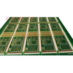
8 Layer HDI PCB Board , Finished Board Thickness 1.6MM , FR4
Material
8 Layer HDI PCB
PCB Specifications:
Layer Count: 8Layer HDI PCB
Board Thickness: 1.6MM
Material: FR4
Min Hole: 0.1MM
Min Line: 3/3 Mil
BGA Size: 10Mil
Unit Size: 92*78mm/4up
Hole: L1-L2, L2-L7, L7-L8, L1-L8
Solder Mask: Green
Surface Treatment: ENIG
Application: Camera
Capabilities:
| Item | Capability |
| Layer Count | 1-24 Layers |
| Board Thickness | 0.1mm-6.0mm |
| Finished Board Max Size | 700mm* 800mm |
| Finished Board Thickness Tolerance | +/-10% +/-0.1(<1.0mm) |
| Warp | <0.7% |
| Major CCL Brand | KB/NanYa/LTEQ/ShengYi/Rogers Etc |
| Material Type | FR4,CEM-1,CEM-3,Aluminum,Copper,Ceramic, PI, PET |
| Drill Hole Diameter | 0.1mm-6.5mm |
| Out Layer Copper Thickness | 1/20Z-8OZ ; |
| Inner Layer Copper Thickness | 1/3OZ-6OZ |
| Aspect Ratio | 10:1 |
| PTH Hole Tolerance | +/-3mil |
| NPTH Hole Tolerance | +/-1mil |
| Copper Thickness Of PTH Wall | >10mil(25um) |
| Line Width And Space | 2/2mil |
| Min Solder Mask Bridge | 2.5mil |
| Solder Mask Alignment Tolerance | +/-2mil |
| Dimension Tolerance | +/-4mil |
| Max Gold Thickness | 200u'(0.2mil) |
| Thermal Shock | 288C, 10s, 3 Times |
| Impedance Contro | +/-10% |
| LTest Capability | PAD Size Min 0.1mm |
| Min BGA | 7mil |
| Surface Treatment | OSP, ENIG, HASL, Plating Gold, Carbon Oil,Peelable |
FAQ:
Question: What is the standard format you accept?
Answer: We accept standard gerber format file.
Question: Do you accept sample orders?
Answer: YES, we do accept sample orders.
Question: What is the difference between your two factories?
Answer: The HuiZhou factory mainly produce sample and small batch
pcbs. The JiangXi factory has more roboticized equipments, so it
prefers big batch production.
Question: What is a High-Density Interconnect PCB?
Answer: HDI stands for ‘High Density Interconnects’. An HDI PCB is
a dense version of a printed circuit board where the components are
placed closer to each other allowing the overall board size to be
smaller. HDI printed circuit boards use optimized routing, smaller
components, BGA component footprints and optimized vias to make
connections between the components on the board.
In regular PCBs we use through hole vias to connect multiple layers of the board to each other. A
traditional via goes from the top of the PCB to the bottom,
connecting all the layers, as seen in the image below. These vias
are easy to deploy as they can be drilled through the board from
top to bottom using a regular drill. The main disadvantage of
regular vias from a space optimization point of view is that this
via will connect all the layers of the board, even those that do
not need to be connected to each other and thus can result in
wastage of space within some layers of the PCB.
An HDI PCB uses different types of vias – microvias, buried vias
and blind vias to optimize the space requires for interconnections
between the layers and components.

Microvias are ultra-small vias which can be drilled using lasers. They are
much smaller in diameter than regular vias.
A Blind via connects the outer layer to an inner layer, with access to only
one external layer.
A Buried via can connect inner layers of the same substrate or
multiple substrates, with no access to external layers as seen
below.
Blind or buried via gives access to only functionally required
layers, and as a result do not occupy space on all the layers at a
given time. This provides more space for components with enhanced
routing within the traces. A designer can mount more components to
increase the board density or can reduce the board size as per the
requirement.
Advantages of an HDI PCB Board:
- HDI PCBs allow for increased component placements on both sides of
the PCB thereby making the board smaller and lighter
- HDI PCBs can reduce the amount of laminate material required. This
can result in lower pricing of a board when using a very expensive
laminate material
- HDI boards can improve signal transmission along with a reduction
in signal loss and delays as connection paths are shorter
- Provides better heat dissipation


