Semi-Insulating , Iron-Doped Indium Phosphide Substrate , 4”, Prime
Grade
PAM-XIAMEN manufactures high purity single crystal Indium Phosphide
Wafers for optoelectronics applications. Our standard wafer
diameters range from 25.4 mm (1 inch) to 200 mm (6 inches) in size;
wafers can be produced in various thicknesses and orientations with
polished or unpolished sides and can include dopants. PAM-XIAMEN
can produce wide range grades: prime grade, test grade, dummy
grade, technical grade, and optical grade. PAM-XIAMEN also offer
materials to customer specifications by request, in addition to
custom compositions for commercial and research applications and
new proprietary technologies.
Semi-Insulating, Indium Phosphide Substrate, 4”, Prime Grade
| 4"InP Wafer Specification | | | |
| Item | Specifications |
| Conduction Type | SI-type |
| Dopant | Iron |
| Wafer Diameter | 4" |
| Wafer Orientation | 100±0.5° |
| Wafer Thickness | 600±25um |
| Primary Flat Length | 16±2mm |
| Secondary Flat Length | 8±1mm |
| Carrier Concentration | ≤3x1016cm-3 | (0.8-6)x1018cm-3 | (0.6-6)x1018cm-3 | N/A |
| Mobility | (3.5-4)x103cm2/V.s | (1.5-3.5)x103cm2/V.s | 50-70cm2/V.s | >1000cm2/V.s |
| Resistivity | N/A | N/A | N/A | >0.5x10⁷Ω.cm |
| EPD | <1000cm-2 | <1x103cm-2 | <1x103cm-2 | <5x103cm-2 |
| TTV | <15um |
| BOW | <15um |
| WARP | <15um |
| Laser Marking | upon request |
| Suface Finish | P/E, P/P |
| Epi Ready | yes |
| Package | Single wafer container or cassette |
What is InP wafer?
Indium phosphide is a semiconducting material similar to GaAs and
silicon but is very much a niche product. It’s very effective at
developing very high-speed processing and is more expensive than
GaAs because of the great lengths to gather and develop the
ingredients. Let’s take a look at some more facts about indium
phosphide as it pertains to an InP Wafer.
 | Electron Hall mobility versus temperature for different doping
levels.
Bottom curve - no=Nd-Na=8·1017 cm-3;
Middle curve - no=2·1015 cm-3;
Top curve - no=3·1013 cm-3.
(Razeghi et al. [1988]) and (Walukiewicz et al [1980]). |
 | Electron Hall mobility versus temperature (high temperatures):
Bottom curve - no=Nd-Na~3·1017 cm-3;
Middle curve - no~1.5·1016 cm-3;
Top curve - no~3·1015 cm-3.
(Galavanov and Siukaev[1970]). |
For weakly doped n-InP at temperatures close to 300 K electron
drift mobility:
µn = (4.2÷5.4)·103·(300/T) (cm2V-1 s-1)
 | Hall mobility versus electron concentration for different
compensation ratios.
θ = Na/Nd, 77 K.
Dashed curves are theoretical calculations: 1. θ = 0; 2. θ = 0.2;
3. θ = 0.4; 4. θ = 0.6; 5. θ = 0.8;
(Walukiewicz et al. [1980]).
Solid line is mean observed values (Anderson et al. [1985]). |
 | Hall mobility versus electron concentration for different
compensation ratios
θ =Na/Nd, 300 K.
Dashed curves are theoretical calculations: 1. θ = 0; 2. θ = 0.2;
3. θ = 0.4; 4. θ = 0.6; 5. θ = 0.8;
(Walukiewicz et al. [1980]).
Solid line is mean observed values (Anderson et al. [1985]). |
Approximate formula for electron Hall mobility
µ=µOH/[1+(Nd/107)1/2],
where µOH=5000 cm2V-1 s-1,
Nd- in cm-3 (Hilsum [1974])
At 300 K, the electron Hall factor rn≈1 in n-InP.
for Nd > 1015 cm-3.
 | Hole Hall mobility versus temperature for different doping (Zn)
levels.
Hole concentration at 300 K: 1. 1.75·1018 cm-3; 2. 3.6·1017 cm-3;
3. 4.4·1016 cm-3.
θ=Na/Nd~0.1.
(Kohanyuk et al. [1988]). |
For weakly doped p-InP at temperature close to 300 K the Hall
mobility
µpH~150·(300/T)2.2 (cm2V-1 s-1).
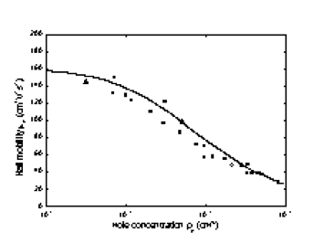 | Hole Hall mobility versus hole density, 300 K (Wiley [1975]).
The approximate formula for hole Hall mobility:
µp=µpo/[1 + (Na/2·1017)1/2], where µpo~150 cm2V-1 s-1, Na- in cm-3 |
At 300 K, the hole factor in pure p-InP: rp~1
Optical Sensing application
Spectroscopic Sensing aiming environmental protection and
identification of dangerous substances
• A growing field is sensing based on the wavelength regime of InP.
One example for Gas Spectroscopy is drive test equipment with
real-time measurement of (CO, CO2, NOX [or NO + NO2]).
• Another example is FT-IR-Spectrometer VERTEX with a terahertz
source. The terahertz radiation is generated from the beating
signal of 2 InP lasers and an InP antenna that transforms the
optical signal to the terahertz regime.
• Stand-Off detection of traces of explosive substances on
surfaces, e.g. for safety applications on airports or crime scene
investigation after assassination attempts.
• Quick verification of traces of toxic substances in gases and
liquids (including tap water) or surface contaminations down to the
ppb level.
• Spectroscopy for non-destructive product control of e.g. food
(early detection of spoiled foodstuff)
• Spectroscopy for many novel applications, especially in air
pollution control are being discussed today and implementations are
on the way.
Are You Looking for an InP Wafer?
PAM-XIAMEN is your go-to place for everything wafers, including InP
wafers, as we have been doing it for almost 30 years! Enquire us
today to learn more about the wafers that we offer and how we can
help you with your next project. Our group team is looking forward
to providing both quality products and excellent service for you!


