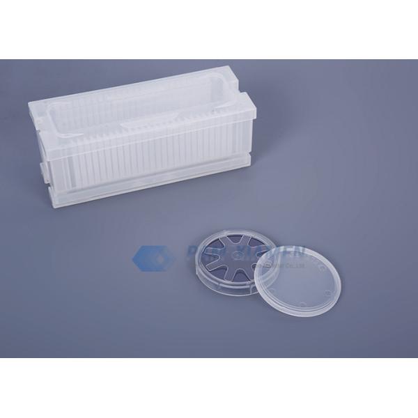
Semi-Insulating ,InP ( Indium Phosphide) Crystal Wafer , 3”, Dummy
Grade
PAM-XIAMEN offers InP wafer – Indium Phosphide which are grown by
LEC(Liquid Encapsulated Czochralski) or VGF(Vertical Gradient
Freeze) as epi-ready or mechanical grade with n type, p type or
semi-insulating in different orientation(111)or(100).
Indium phosphide (InP) is a binary semiconductor composed of indium
and phosphorus. It has a face-centered cubic (“zinc blende”)
crystal structure, identical to that of GaAs and most of the III-V
semiconductors.Indium phosphide can be prepared from the reaction
of white phosphorus and indium iodide[clarification needed] at 400
°C.,[5] also by direct combination of the purified elements at high
temperature and pressure, or by thermal decomposition of a mixture
of a trialkyl indium compound and phosphide. InP is used in
high-power and high-frequency electronics[citation needed] because
of its superior electron velocity with respect to the more common
semiconductors silicon and gallium arsenide.
Semi-Insulating, InP Wafer, 3”, Dummy Grade
| 3"InP Wafer Specification | | | |
| Item | Specifications |
| Conduction Type | SI-type |
| Dopant | Iron |
| Wafer Diameter | 3" |
| Wafer Orientation | 100±0.5° |
| Wafer Thickness | 600±25um |
| Primary Flat Length | 16±2mm |
| Secondary Flat Length | 8±1mm |
| Carrier Concentration | ≤3x1016cm-3 | (0.8-6)x1018cm-3 | (0.6-6)x1018cm-3 | N/A |
| Mobility | (3.5-4)x103cm2/V.s | (1.5-3.5)x103cm2/V.s | 50-70cm2/V.s | >1000cm2/V.s |
| Resistivity | N/A | N/A | N/A | >0.5x10⁷Ω.cm |
| EPD | <1000cm-2 | <500cm-2 | <1x103cm-2 | <5x103cm-2 |
| TTV | <12um |
| BOW | <12um |
| WARP | <15um |
| Laser Marking | upon request |
| Suface Finish | P/E, P/P |
| Epi Ready | yes |
| Package | Single wafer container or cassette |
What is the InP Process?
InP wafers must be prepared prior to device fabrication. To start,
they must be completely cleaned to remove any damage that might
have occurred during the slicing process. The wafers are then
Chemically Mechanically Polished/Plaranrized (CMP) for the final
material removal stage. This allows for the attainment of
super-flat mirror-like surfaces with a remaining roughness on an
atomic scale. After that is completed, the wafer is ready for
fabrication.
Basic Parameters
| Breakdown field | ≈5·105 V cm-1 |
| Mobility electrons | ≤5400 cm2V-1s-1 |
| Mobility holes | ≤200 cm2 V-1s-1 |
| Diffusion coefficient electrons | ≤130 cm2 s-1 |
| Diffusion coefficient holes | ≤5 cm2 s-1 |
| Electron thermal velocity | 3.9·105 m s-1 |
| Hole thermal velocity | 1.7·105 m s-1 |
Telecom/Datacom Application
Indium Phosphide (InP) is used to produce efficient lasers,
sensitive photodetectors and modulators in the wavelength window
typically used for telecommunications, i.e., 1550 nm wavelengths,
as it is a direct bandgap III-V compound semiconductor material.
The wavelength between about 1510 nm and 1600 nm has the lowest
attenuation available on optical fibre (about 0.26 dB/km). InP is a
commonly used material for the generation of laser signals and the
detection and conversion of those signals back to electronic form.
Wafer diameters range from 2-4 inches.
Applications are:
• Long-haul optical fibre connections over great distance up to
5000 km typically >10 Tbit/s
• Metro ring access networks
• Company networks and data center
• Fibre to the home
• Connections to wireless 3G, LTE and 5G base stations
• Free space satellite communication
Are You Looking for an InP substrate?
PAM-XIAMEN is proud to offer indium phosphide substrate for all
different kinds of projects. If you are looking for InP wafers,
send us enquiry today to learn more about how we can work with you
to get you the InP wafers you need for your next project. Our group
team is looking forward to providing both quality products and
excellent service for you!
 Crystal Wafer , 3”, Dummy Grade on sale")
 Crystal Wafer , 3”, Dummy Grade on sale")