Truth Instruments Co., Ltd. is a cutting-edge high-tech
enterprise specializing in the research, development, production, and sales of high-end
scientific research instruments and integrated circuit production
line testing equipment. The company's core mission is to empower
technological innovation through the provision of precision
measurement instruments. Against the backdrop of the rapid development of the global integrated circuit manufacturing industry and related fields such
as materials, nanotechnology, and semiconductors, Truth Instruments has launched engineering efforts to develop relevant high-end instruments and equipment through self-innovation,
industry-academia-research cooperation, and technological transformation, and aspires to achieve a position as a world-class leader in the
instrumentation sector.
Since its establishment in 2019, the company has gathered over 150 talented individuals, forming a comprehensive engineering team
specializing in optics, electronics, precision mechanics,
measurement and control, automation, software, algorithms, and
more. Headquartered in Qingdao, China, with subsidiary operations
in Beijing and Hangzhou, the company is strategically positioned
within key technological hubs.
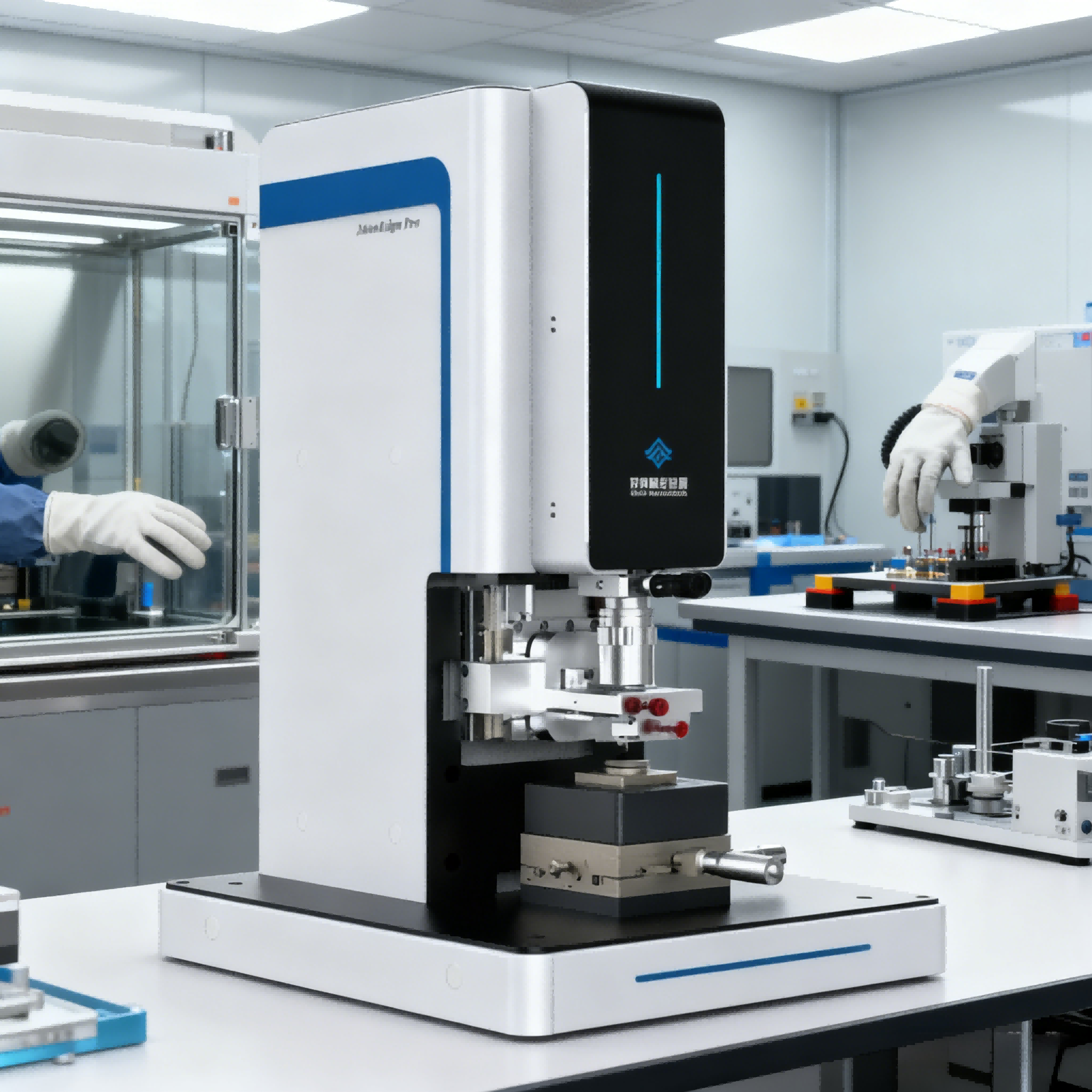
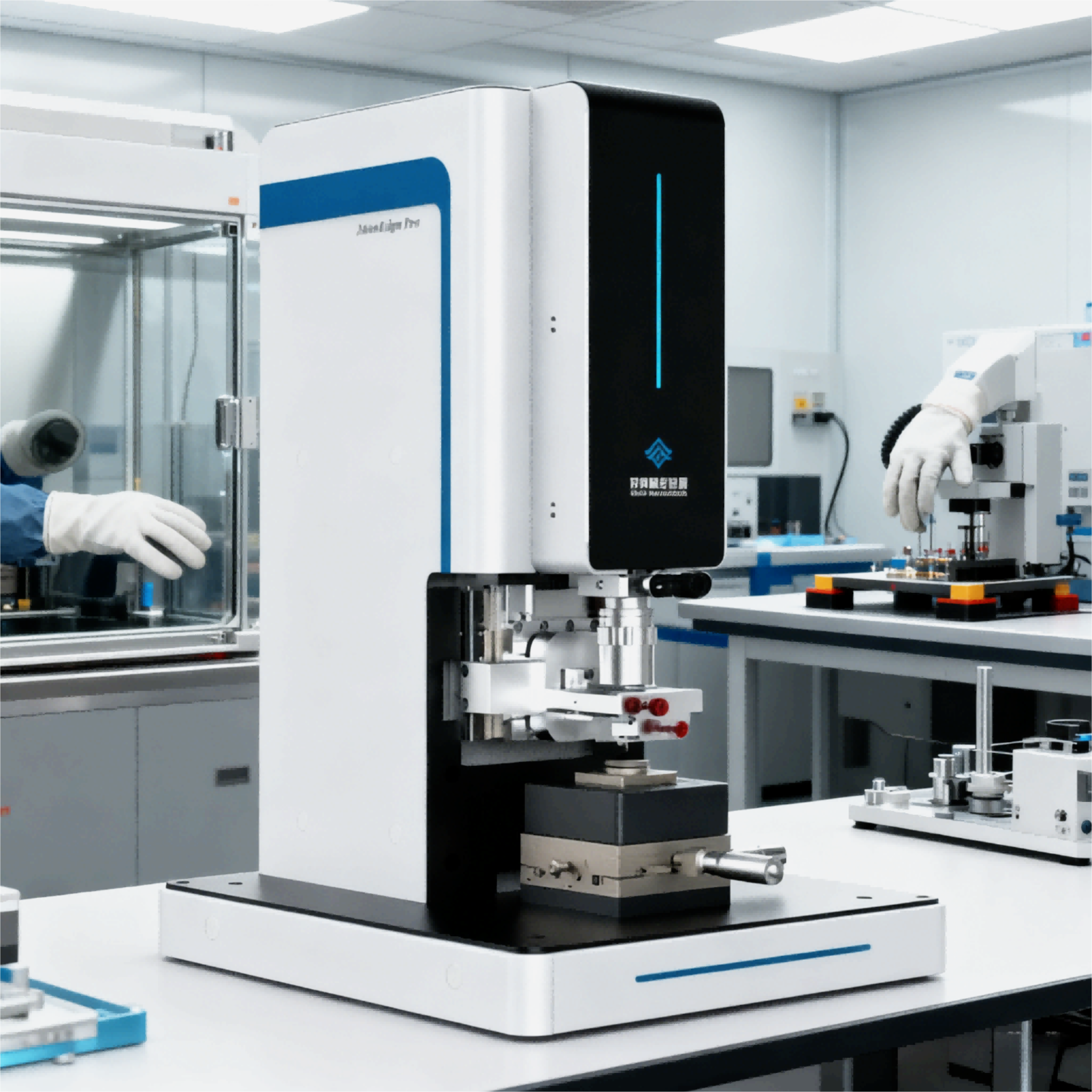
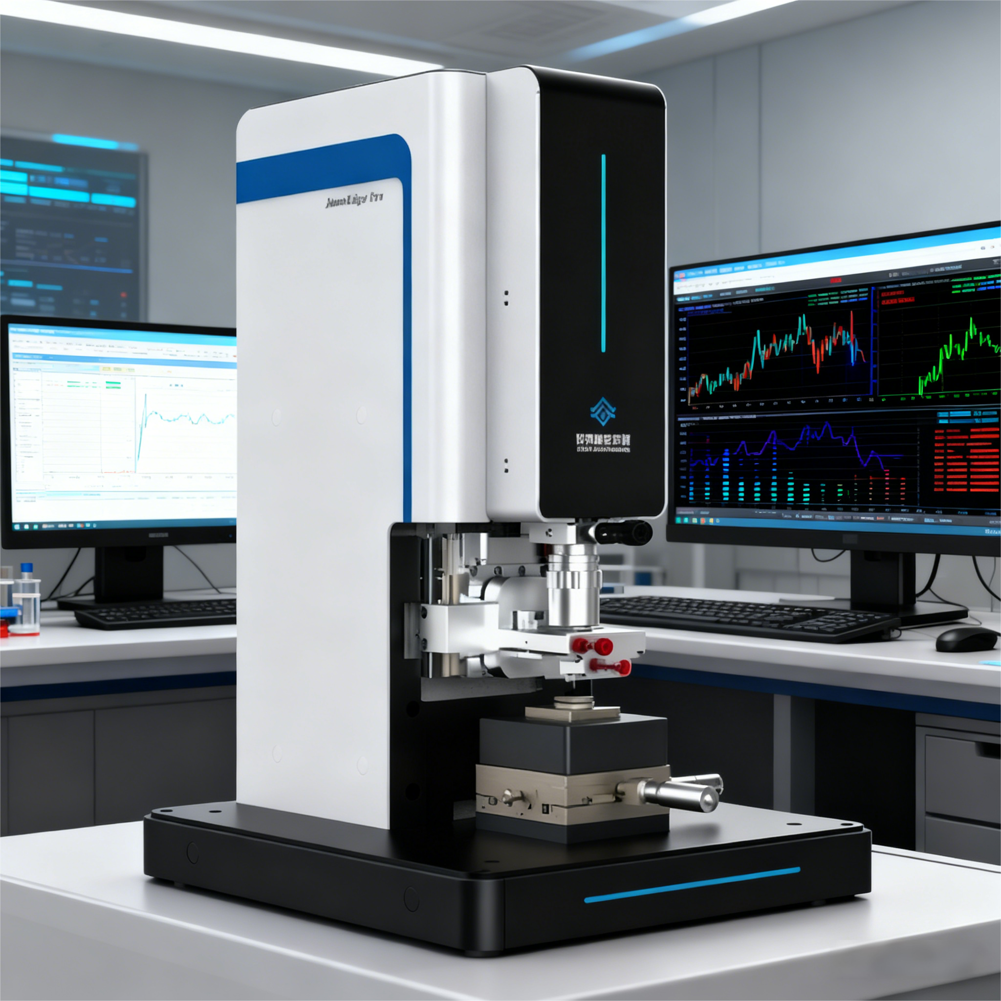
Currently, the company has developed a series of high-end instruments and equipment to meet the demand for high-performance and high-quality devices from researchers and industrial workers. These include "atomic force microscopes,
high-precision VSM, MOKE, and other magnetic measurement devices,
various magnetic field probe stations, magnetic chip CP testing machine and other production-level equipment, cryogenic equipment, etc." The products have been applied in top research institutions, as
well as well-known industrial companies.
Truth Instruments possesses strong independent research and innovation
capabilities, with stable and high-quality products that have
repeatedly supported researchers and industrial workers in
achieving high-level work outcomes. We look forward to
collaborating with more outstanding researchers and industrial
workers from the world to provide more professional technical services and comprehensive
industry solutions! Feel free to contact us!