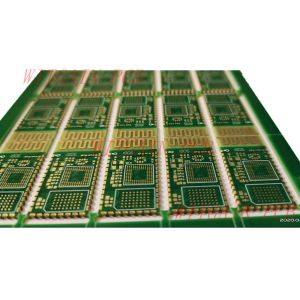
6 Layer Printed Circuit Board With Blind And Buried Holes
PCB Specifications:
Layer Count: 6Layer HDI PCB
Board Thickness: 0.6MM
Material: FR4 TG150
Holes: L1-L2 0.1MM, L2-L5 0.15MM, L5-L6 0.1MM, L1-L6 0.5MM
Min Line: 3.5/2.8 Mil
BGA Size: 12Mil
Unit Size: 113.42MM*92.88MM/6UP
Blind Holes: L1-L2 , L5-L6 0.1MM
Buried Holes: L2-L5 0.13MM
Solder Mask: Black
Surface Treatment: ENIG+OSP
Application: Mobile Phone Charging Board
Our Manufacturing Capabilities:
| NO | Item | Capability |
| 1 | Layer Count | 1-24 Layers |
| 2 | Board Thickness | 0.1mm-6.0mm |
| 3 | Finished Board Max Size | 700mm*800mm |
| 4 | Finished Board Thickness Tolerance | +/-10% +/-0.1(<1.0mm) |
| 5 | Warp | <0.7% |
| 6 | Major CCL Brand | KB/NanYa/ITEQ/ShengYi/Rogers Etc |
| 7 | Material Type | FR4,CEM-1,CEM-3,Aluminum,Copper, Ceramic, PI, PET |
| 8 | Drill Hole Diameter | 0.1mm-6.5mm |
| 9 | Out Layer Copper Thickness | 1/2OZ-8OZ |
| 10 | Inner Layer Copper Thickness | 1/3OZ-6OZ |
| 11 | Aspect Ratio | 10:1 |
| 12 | PTH Hole Tolerance | +/-3mil |
| 13 | NPTH Hole Tolerance | +/-1mil |
| 14 | Copper Thickness of PTH Wall | >10mil(25um) |
| 15 | Line Width And Space | 2/2mil |
| 16 | Min Solder Mask Bridge | 2.5mil |
| 17 | Solder Mask Alignment Tolerance | +/-2mil |
| 18 | Dimension Tolerance | +/-4mil |
| 19 | Max Gold Thickness | 200u'(0.2mil) |
| 20 | Thermal Shock | 288℃, 10s, 3 times |
| 21 | Impedance Control | +/-10% |
| 22 | Test Capability | PAD Size min 0.1mm |
| 23 | Min BGA | 7mil |
| 24 | Surface Treatment | OSP, ENIG,HASL, Plating Gold, Carbon Oil,Peelable Mask etc |
FAQ:
Question: What are solder beads? How are they formed?
Answer:

Solder Beads are balls of solder that are created when soldering
components on a PCB. They are created due to the use of excessive
solder paste when soldering components on a board. Solder beads can
cause a short circuit between the component terminals which can
result in failure of the circuit. Also, in case there are
vibrations, the solder ball can break loose and cause a short
circuit somewhere else on the PCB. This is an undesirable
phenomenon or defect in SMT (Surface Mount Technology).
Due to the solder beads, there may be a chance of occurrence of an
electrical short circuit between terminals of chip resistors or
capacitors or ICs where it was formed. Also, if any vibration in
PCB due to any reason, there may be a chance of the solder bead to
break loose and move across PCB and make short circuits anywhere on
the board. It is an undesirable phenomenon or defect in SMT.
How does solder beading occur?
The pads of PCB contain the solder paste. The required components
(Chip Resistor, Capacitors or other IC) of a circuit are placed on
the corresponding pads, and the PCB is sent into the reflow oven.
In the reflow oven due to heat, the solder paste starts to
melt-down. If there is excessive solder paste, some solder paste
separates from the main solder paste on the pads and ends up
underneath the component.

Solder stuck underneath the component
The solder stuck underneath the component does not return to solder
pads and tends to form a ball of solder also known as a solder
bead. During the cooling process, the surface tension of the
cooling solder pulls the component closer to the pads. Here, the
component is drawn down, towards the board and as a result the
solder squeezes out on the side of the component in the form of a
bead or ball.

Solder bead squeezes out the side of the component and remains
there
How to prevent solder bead formation?
Manual removal of solder removal is expensive and impractical. It
is better to eliminate the solder beads before they occur. Since
solder beading is usually caused by the use of excessive solder
paste on the pads, the best solution would be to reduce the amount
of solder paste being applied to the pads. This can be done by
using the following ways:
1. Increasing Stencil Thickness
2. Modifying Aperture shape/size
3. Changing viscosity of the Solder paste
4. Adjusting the reflow profile
5. Modifying the Squeegee speed and pressure
What causes for Solder beading formation?
Solder beading is caused by the use of excessive solder paste on
the solder pads of a PCB. Other factors include the closeness of
pads on a PCB, the shape of the pads, the reflow or melting profile
used, and environmental conditions.


