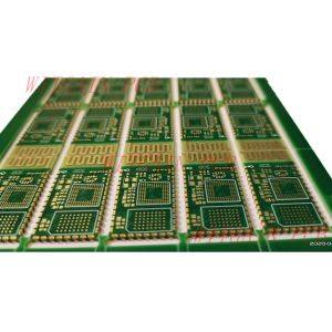
4 Layer Printed Circuit Board With Blind Holes
PCB Specifications:
Layer Count: 4Layer HDI PCB
Board Thickness: 1.6MM
Material: FR4 TG150
Copper Thickness: 1/H/H/1OZ
Min Hole: 0.1MM
Blind Holes: L1-L2 0.1MM
Via Holes: L1-L4 0.2MM
Min Line: 6/8 Mil
BGA Size: 8.5Mil
Unit Size: 100M*110MM/6UP
Solder Mask: Black
Surface Treatment: Immersion Gold
Capabilities:
| Item | Capability |
| Layer Count | 1-24 Layers |
| Board Thickness | 0.1mm-6.0mm |
| Finished Board Max Size | 700mm* 800mm |
| Finished Board Thickness Tolerance | +/-10% +/-0.1(<1.0mm) |
| Warp | <0.7% |
| Major CCL Brand | KB/NanYa/LTEQ/ShengYi/Rogers Etc |
| Material Type | FR4,CEM-1,CEM-3,Aluminum,Copper,Ceramic, PI, PET |
| Drill Hole Diameter | 0.1mm-6.5mm |
| Out Layer Copper Thickness | 1/20Z-8OZ ; |
| Inner Layer Copper Thickness | 1/3OZ-6OZ |
| Aspect Ratio | 10:1 |
| PTH Hole Tolerance | +/-3mil |
| NPTH Hole Tolerance | +/-1mil |
| Copper Thickness Of PTH Wall | >10mil(25um) |
| Line Width And Space | 2/2mil |
| Min Solder Mask Bridge | 2.5mil |
| Solder Mask Alignment Tolerance | +/-2mil |
| Dimension Tolerance | +/-4mil |
| Max Gold Thickness | 200u'(0.2mil) |
| Thermal Shock | 288C, 10s, 3 Times |
| Impedance Contro | +/-10% |
| LTest Capability | PAD Size Min 0.1mm |
| Min BGA | 7mil |
| Surface Treatment | OSP, ENIG, HASL, Plating Gold, Carbon Oil,Peelable |
FAQ:
Quesion: What is Soak Testing or Endurance Testing of a PCB Board?
Answer: Soak Testing also known as Load Testing or Endurance
testing is test performed to check the stability of the PCB over
various extreme operating conditions for extended periods of time.
For example, a PCB board may perform normally when used for 2
hours, but when the same board is used for 10 hours or more than
that, then it may fail. Soak Testing is done to evaluate how the
board will operate under different operating conditions for
extended periods of time. Soak Testing should be done before the
final deployment of the board.
Question: What is PCB Grid Testing or Bed of Nails Testing?
Answer: Grid testing or Bed of Nails testing is a process used to
check the performance of components mounted on a PCB board. This
test uses a frame/fixture that contains various pins inserted into
an epoxy phenolic glass cloth laminated sheet (G-10) in order to
access all the PCB test points. These pins act as sensors which are
aligned to make contact with the test points on the PCB board and
are also connected with a measuring unit through wires. The
position of the pins is designed and customized for each PCB based
on the components or points on the board that need to be tested.

A grid testing machine has three building blocks - a fixture, a bed
of nails and software, to control the overall functionality of the
machine. It usually has two cameras which are placed on the top and
bottom of the machine in order to scan the whole board.
Advantages of PCB Grid Testing:
- Very Reliable method of PCB testing as all the points on the PCB
board can be tested simultaneously.
- Offers very good accuracy since it uses two cameras
- Can easily detect manufacturing defects
- An in-circuit tester is easy to program
- Interpretation of test results is quite easy
- It checks for Open, shorts, mission components, Wrong polarity,
defective components, and current leakages in the circuit
- Most of the parameters can be checked without applying power to the
PCB under test
Limitations of PCB Grid Testing:
- Fixtures used in bed of nails testing are expensive since they are
mechanical and require a different wiring assembly for a different
PCB board
- Fixtures are mechanical so any change in the number of pins or
their position require extra cost
- This test doesn’t test continuity through connectors so there are
the chances that the connectors’ faults may remain unnoticed.
- Faults related to solder joints, excess solder, solder quality, and
solder void also remain unidentified
This type of testing is called In-Circuit Testing. Another test
process used for In-Circuit testing is Flying Probe Testing.


