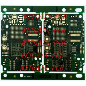
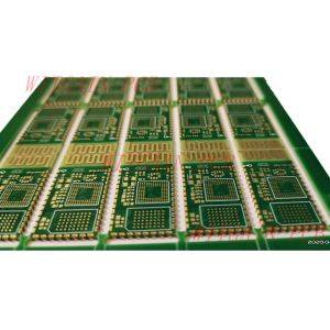
10 Layer HDI PCB, FR4, TG170, ENIG, Laser Drilling , Blind And
Buried Holes
10 Layer HDI Printed Circuit Board With Blind And Buried Holes
PCB Specifications:
Layer Count: 10 Layer HDI PCB
Board Thickness: 1.6MM
Material: FR4 High TG
Min Hole: 0.1MM
Min Line: 3/3 Mil
Hole: L1-L2, L2-L3, L3-L8, L8-L9, L9-10, L1-L10
Solder Mask: Green
Surface Treatment: ENIG
Application: Industrial Power Supply Products
About Us
We have about 300 employees in two factories and the monthly output
is around 30000m2. Our marketing orientation is to make high
difficult and special treatment pcb. Even though, we still accept
normal 2-layer and multi-layer pcb orders. Our products cover
simple double layer pcb, multi-layer pcb, HDI pcb, rigid-flex pcb,
fpc, ceramic pcb, heavy gold/copper pcb etc. Wide product ranges
and flexible order quantities allow us to satisfy most customer's
demands.
Capabilities:
| Item | Capability |
| Layer Count | 1-24 Layers |
| Board Thickness | 0.1mm-6.0mm |
| Finished Board Max Size | 700mm* 800mm |
| Finished Board Thickness Tolerance | +/-10% +/-0.1(<1.0mm) |
| Warp | <0.7% |
| Major CCL Brand | KB/NanYa/LTEQ/ShengYi/Rogers Etc |
| Material Type | FR4,CEM-1,CEM-3,Aluminum,Copper,Ceramic, PI, PET |
| Drill Hole Diameter | 0.1mm-6.5mm |
| Out Layer Copper Thickness | 1/20Z-8OZ ; |
| Inner Layer Copper Thickness | 1/3OZ-6OZ |
| Aspect Ratio | 10:1 |
| PTH Hole Tolerance | +/-3mil |
| NPTH Hole Tolerance | +/-1mil |
| Copper Thickness Of PTH Wall | >10mil(25um) |
| Line Width And Space | 2/2mil |
| Min Solder Mask Bridge | 2.5mil |
| Solder Mask Alignment Tolerance | +/-2mil |
| Dimension Tolerance | +/-4mil |
| Max Gold Thickness | 200u'(0.2mil) |
| Thermal Shock | 288C, 10s, 3 Times |
| Impedance Contro | +/-10% |
| LTest Capability | PAD Size Min 0.1mm |
| Min BGA | 7mil |
| Surface Treatment | OSP, ENIG, HASL, Plating Gold, Carbon Oil,Peelable |
FAQ:
Questions: How many lamination times for this 10 Layer HDI PCB?
Answer: For this PCB, there are 3 times lamination in total.
Questions: What is the normal lead time for this kind of PCB?
Answer: The standard lead time for sample is about 3 weeks, for
production is about 4 weeks. It may fluctuate according to
production and orders status.
Quesions: What are fiducial marks or non-fading marks on a printed circuit
board?
Answer:
Fiducial marks are recognition marks, created in the form of small pads on the
PCB board to act as reference points for PCB Stencil alignment and
for automated component placement by Pick and Place machines.
During the PCB Assembly process these points are used by automated
machines to ensure correct positioning of the board. These points
are also measurable and act as a frame of reference during SMT
component placement.
When an operator loads the PCB board for printing or component
placement, the machine identifies the fiducial marks on the PCB and
uses image recognition to match the exact location. This way, the
automatic machine aligns itself based on the fiducial marks.
The addition of fiducial marks is a part of PCB circuit artwork. It
means that the PCB circuit pattern and fiducial marks should be
etched at the same step. The desired base material of the fiducial
mark should be copper protected by an anti-oxidation coating. The
fiducial locations are added to the stencil and pick & drop data
file.
It is always recommended to create three fiducial marks on the PCB
since it helps the automated machine to identify whether the board
is loaded in the right direction or not. Two fiducial marks are
also acceptable.

Types of Fiducial marks:
There are two types of fiducial marks available based on their
location on the PCB board:
- Global Fiducial Marks: They are created to differentiate the PCB circuit pattern from the
panel datum. They should be located based on three point grid
system, where the lower left fiducial is located at the 0,0 point
while the other two at the positive X and Y axis. Also, called
panel fiducial, if multiple boards are required to be processed at
the same time.
- Local Fiducial Marks: These marks are used to locate the position of an individual
component that requires more precision.
Key Guidelines for creating fiducial marks on a PCB:
While adding the fiducial marks, the following points should be
considered:
- These marks should be added only on the top or bottom copper layers
of the PCB.
- They should not be covered by the solder mask since the automated
system needs to identify them and covering the same with solder
mask will make it impossible to track.
- For better performance, a high degree of contrast between the
surface of the fiducial mark and the adjacent PCB board base
material is desired.
- Usually, the fiducial marks are round in shape, but square or
diamond shapes are also acceptable.
- To achieve better precision, the fiducial marks should be placed as
far from each other as possible on the PCB.
- The diameter of a fiducial mark should lie between 1 mm (0.040 in)
to 3 mm (0.120 in). The marks on the same PCB should not vary in
size by more than 25 microns (0.001 in).
Exhibitions:


